THERMAL/PHOTON INSPECTION
Thermal inspection total solution
System introduction
A solution to location defections through a highly-functional thermal camera.
Total Solution is provided by propelling the Display Device to take measurements that can be
adjusted depending on the frequency changes.
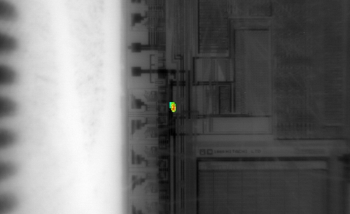
High Power Transistor Measurement
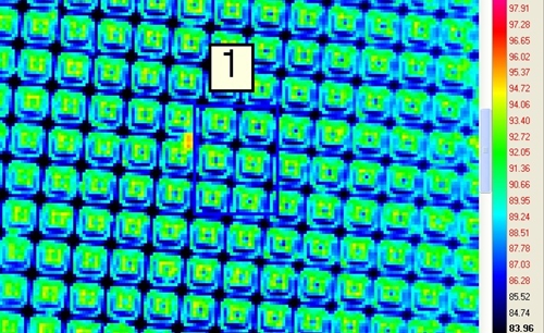
Micro-LED Sample Test
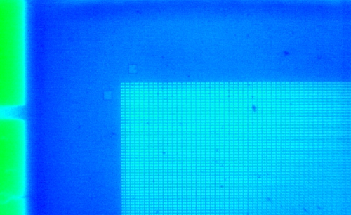
Touch Panel Short Sample Image
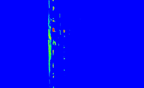
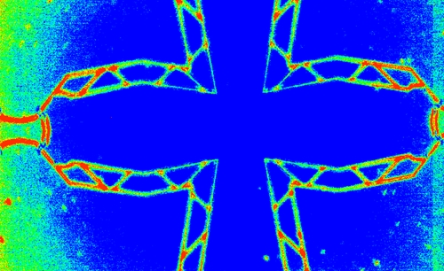
Overlay Image Process
(Marked only Areas with High Level of
Intensity)
Overlay Image Process
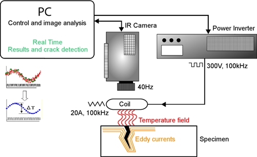
Interface Thermal Lock-in Solution
| Items | Functions | Note |
|---|---|---|
| Camera Spec. | Various detector type and resolution options available according to customers’ requests | Insb Camera |
| Dual Measurement | Able to detect electric properties as well as defections using the Detector Camera | |
| Low - High Magnification | Able to detect low to high magnification according to customers’ requests | 고객과 사양 협의 후 결정 |
| Manual or Auto Mode | Able to measure by probing through recipe if the area to be measured is large | 불량 조건 설정, 측정 후 GUI에 표시 및 저장 |
| Vision Image Processing |
|
|
| Tester and Interface |
|
Detector Camera Tester Interface (H/W or S/W) |
| Other Application Examples |
|
Manual Prober System (Thermal/Photon )
Thermal manual prober System introduction
The Thermal Manual Prober System uses a highly sensitive Thermal Camera that detects interior heating of semiconductor devices. The Thermal Manual Prober System can rapidly and accurately detect semiconductors’ defection locations by displaying detected heat burns in overlapping patterns.
Specification:
- Chuck Size : 200mm
- Chuck Material : Nickel plated
- Stage Stroke : XY Axis(200mm)Z Axis(10mm) , Theta(Fine theta manual movement ± 3°)
- Optic Stage Stroke : XYZ Axis(±50mm)
- Isolation Table : 3 Auto Leveling Valve, Natural Frequency of System : Vertical : 1.2~1.5Hz
- Optic Unit : 4 or 5Hole Turret, Probing View Camera
- Option : Hot Chuck (Temp 200 Celsius)
- Size : (W)960 x (D)985 x (H) 1,800
- Utility : CDA(0.5MPa), Vacuum(50KPa)
Photon manual prober System introduction
The Photon Manual Prober System is a very sustainable system that can measure DC (I-V, C-V) and RF, as well as be utilized in various other areas, which provides accurate probing through an easy operation.
It is possible to measure 200mm and 300mm Wafer Loading and Partial Wafer, and Chip Unit Samples, and provides probing that utilizes the Probe Card and Positioner. Overall, the measurement Tester and Interface support and measurement accessories are provided.
Top Side Manual System is the best Probing System that can be upgraded in various ways through the customer request application.
Specification:
- Chuck Size : 200mm
- Chuck Material : Nickel plated
- Stage Stroke : XY Axis(200mm)Z Axis(10mm) , Theta(Fine theta manual movement ± 3°)
- Optic Stage Stroke : XYZ Axis(±50mm)
- Isolation Table : 3 Auto Leveling Valve, Natural Frequency of System : Vertical : 1.2~1.5Hz
- Optic Unit : 4 or 5Hole Turret, Probing View Camera
- Option : Hot Chuck (Temp 200 Celsius)
- Size : (W)960 x (D)985 x (H) 1,800
- Utility : CDA(0.5MPa), Vacuum(50KPa)