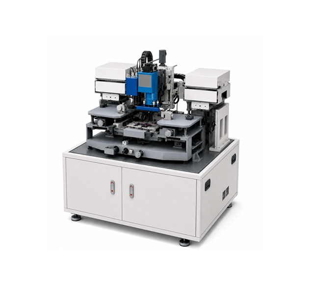
Thermal Emission Probe Station
Thermal Emission Probe Station은 반도체 소자에 전기적 Bias 또는 Stress를 인가하면서 발생하는 미세한 온도 변화 및 국부적인 발열(Hot Spot)을 고감도 IR Camera를 이용하여 검출·분석하는 반도체 Failure Analysis 장비입니다.
반도체 Device에 전압과 전류가 인가되면 정상적인 동작에서도 열이 발생하지만, 불량이나 국부적인 Leakage Current가 존재하는 경우 특정 영역에서 비정상적으로 높은 열이 발생할 수 있습니다.
본 장비는 이러한 Thermal Emission을 비접촉 방식으로 측정하여 발열 위치와 온도 분포를 분석할 수 있습니다.
검출된 열화상 이미지와 소자의 패턴 이미지를 정밀하게 중첩하여 표시함으로써, 불량이 발생한 위치를 빠르고 정확하게 확인할 수 있습니다.
또한 자체 개발 한 Thermal Lock-In System을 이용하여 이를 통해 반도체 및 디스플레이 소자의 전기적 이상 부위와 발열 원인을 효율적으로 분석할 수 있으며, 높은 위치 정밀도를 기반으로 신속한 Failure Analysis를 지원합니다.
Thermal Emission Probe Station
The Thermal Emission Probe Stationuses a high-sensitivity IR camera to detect minute temperature changes and localized hot spots generated under electrical bias or stress.
Devices produce heat during normal operation, but defects or localized leakage can create abnormal hot spots. Non-contact thermal-emission measurement maps the heat source and temperature distribution. Thermal images are precisely overlaid with device-pattern images to locate failures quickly and accurately. A proprietary Thermal Lock-In System further improves sensitivity.
The system efficiently identifies electrical anomalies and heat sources in semiconductor and display devices, supporting rapid failure analysis with high positional accuracy.
주요 적용 분야
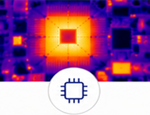
전력 반도체
High Power 소자
열 분포 분석 및 과열 불량 검출
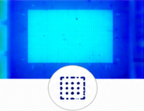
Micro-LED / Display
발광 불량, 휘도 편차 및
불량 영역 검출
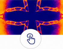
Touch Panel
단략, 개방 불량 및
전극 패턴 이상 검출
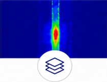
이미지 Overlay
가시광 이미지와 열/광학 이미지
정합 및 결함 강조
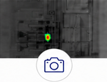
IR Overlay
IR 이미지와 실사 이미지
정합 및 결함 위치 확인
Key Applications
Power Semiconductor
Analyze heat distribution in
high-power devices and detect overheating
Micro-LED / Display
Detect emission defects, shorted areas,
and non-emitting zones
Touch Panel
Detect open, short, and
electrode pattern anomalies
Image Overlay
Align visible and thermal/emission images
to highlight defects
IR Overlay
Align IR and live images
to locate defects
Specification
| Chuck Size | 200mm (10mm~300mm, 디스플레이 Panel 고객 요청에 따라 변경 가능) |
|---|---|
| Probe Type | Double Side Prober (Top, Back) |
| Chuck Material | Nickel plated |
| Stage Stroke | XY Axis(200mm)Z Axis(10mm) , Theta(Fine theta manual movement ± 3°) |
| Optic Stage Stroke | XYZ Axis(±50mm) |
| Isolation Table | 3 Auto Leveling Valve, Natural Frequency of System : Vertical : 1.2~1.5Hz |
| Optic Unit | 4 or 5Hole Turret, Probing View Camera |
| Option | NCF 시스템(미세 열을 감지 하기 위한 I-PRECISION에서 자체 개발) |
| Size | (W)960 x (D)985 x (H) 1,800 |
| Utility | CDA(0.5MPa), Vacuum(50KPa) |
| Chuck Size | 200mm (10mm–300mm or display panels, customizable on request) |
|---|---|
| Probe Type | Double Side Prober (Top, Back) |
| Chuck Material | Nickel plated |
| Stage Stroke | XY Axis(200mm)Z Axis(10mm) , Theta(Fine theta manual movement ± 3°) |
| Optic Stage Stroke | XYZ Axis(±50mm) |
| Isolation Table | 3 Auto Leveling Valve, Natural Frequency of System : Vertical : 1.2~1.5Hz |
| Optic Unit | 4 or 5Hole Turret, Probing View Camera |
| Option | NCF System (I-PRECISION proprietary micro-heat detection) |
| Size | (W)960 x (D)985 x (H) 1,800 |
| Utility | CDA(0.5MPa), Vacuum(50KPa) |