
Photon Emission Probe Station
The Photon Emission Probe Station detects faint photons generated while electrical stress is applied to a semiconductor device. Its high-sensitivity optical system locates leakage current, junction breakdown, hot-carrier effects, gate-oxide failure, ESD damage, and other localized electrical defects.
It correlates emission locations with electrical behavior, revealing internal defects that are difficult to identify through electrical measurement alone.
Photon Emission Probe Station
Photon Emission Probe Station은 반도체 소자에 전기적 스트레스를 인가하면서 발생하는 미세한 광자(Photon)를 고감도 광학 시스템을 이용하여 검출하며, 소자의 Leakage Current, Junction Breakdown, Hot Carrier, Gate Oxide Failure, ESD Damage 및 기타 국부적인 전기적 결함 위치를 분석하는 장비입니다.
일반적인 전기적 측정만으로는 확인하기 어려운 반도체 및 디스플레이 내부의 미세 결함을 Emission 위치와 전기적 특성을 동시에 분석할 수 있다는 장점이 있습니다.
주요 적용 분야는 다음과 같습니다.
Applications include semiconductor failure analysis, wafer-level photon-emission analysis, IC/memory/power semiconductor analysis, leakage-current failures, ESD/EOS failures, gate-oxide breakdown, junction leakage, hot-carrier emission, and process/device reliability development.
주요 적용 분야
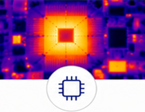
전력 반도체
High Power 소자
열 분포 분석 및 과열 불량 검출
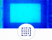
Micro-LED / Display
발광 불량, 휘도 편차 및
불량 영역 검출
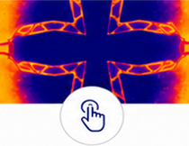
Touch Panel
단략, 개방 불량 및
전극 패턴 이상 검출
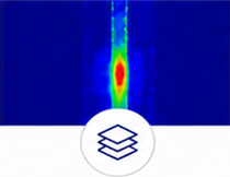
이미지 Overlay
가시광 이미지와 열/광학 이미지
정합 및 결함 강조
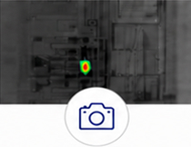
IR Overlay
IR 이미지와 실사 이미지
정합 및 결함 위치 확인
Key Applications
Power Semiconductor
Analyze heat distribution in
high-power devices and detect overheating
Micro-LED / Display
Detect emission defects, shorted areas,
and non-emitting zones
Touch Panel
Detect opens, rework defects,
and electrode abnormalities
Image Overlay
Align visible and thermal/emission images
to highlight defects
IR Overlay
Align IR and live images
to locate defects
Specification
| Chuck Size | 200mm (10mm~300mm, 디스플레이 Panel 고객 요청에 따라 변경 가능) |
|---|---|
| Chuck Material | Nickel plated |
| Stage Stroke | XY Axis(200mm)Z Axis(10mm) , Theta(Fine theta manual movement ± 3°) |
| Optic Stage Stroke | XYZ Axis(±50mm) |
| Isolation Table | 3 Auto Leveling Valve, Natural Frequency of System : Vertical : 1.2~1.5Hz |
| Optic Unit | 4 or 5Hole Turret, Probing View Camera |
| Option | Hot Chuck (Temp 200 Celsius) |
| Size | (W)960 x (D)985 x (H) 1,800 |
| Utility | CDA(0.5MPa), Vacuum(50KPa) |
| Chuck Size | 200mm (10mm–300mm or display panels, customizable on request) |
|---|---|
| Chuck Material | Nickel plated |
| Stage Stroke | XY Axis(200mm)Z Axis(10mm) , Theta(Fine theta manual movement ± 3°) |
| Optic Stage Stroke | XYZ Axis(±50mm) |
| Isolation Table | 3 Auto Leveling Valve, Natural Frequency of System : Vertical : 1.2~1.5Hz |
| Optic Unit | 4 or 5Hole Turret, Probing View Camera |
| Option | Hot Chuck (Temp 200 Celsius) |
| Size | (W)960 x (D)985 x (H) 1,800 |
| Utility | CDA(0.5MPa), Vacuum(50KPa) |